| HOME |
| CUSTOM DESIGN |
| PRODUCTS |
| CONTACT |
| CIRCUITS |
| FAQs |
| RESOURCES |
| LINKS |
| ABOUT |
For other 7400 series TTL IC
datasheets, CLICK HERE
|
Always check pinouts before wiring any IC, some manufacturers' designs may vary.
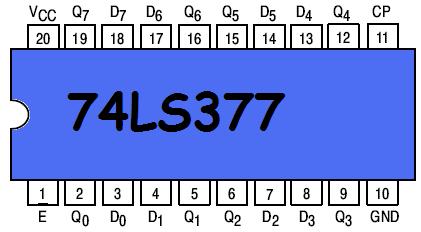
| The 74LS377
(74377) IC
contains eight general purpose D flip-flop circuits with a buffered
common clock input a buffered common clock enable pin. When configured
(externally wired), data present on the chip's input pins will be
transfered and latched to the chip's output pins upon receiving a clock
signal. Subsequent reconfiguring of the input values will have no
effect until another clock pulse is received. The 74377 is useful as a general purpose 8-bit register and is commonly found in multiplexed digital display drivers to hold intermittent states until new data must be transfered, especially in systems where the output bus contains only enough pins to drive a single 7-segment display. By wiring the inputs of many 74377s together in parallel, a microcontroller, for instance, can select the desired 8-bit register (target) and write data to each one at a time, as long as separate lines are dedicated for each 74377's clock input or enable pin. As an example, with the use of only 16 microcontroller / microprocessor I/O lines, 8 seven segment displays can be driven (flicker free, since the 74377 provides latching). 8 lines would be used for the data inputs (to all of the chips) and the other 8 to select which of the 8 chips receives the data. Of course, a line decoder can provide additional benefit by allowing the processor to select the desired chip through a binary decoding. |
See
74LS378 for the 6 Latch Version
See 74LS379 for the 4 Latch Version |
| View
Datasheet Immediately -
CLICK HERE |
|
Internal logic of the 74377 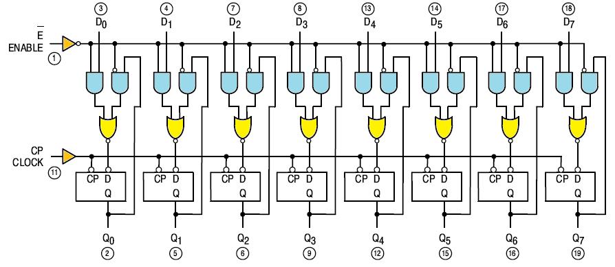 |
Features: •8-Bit High Speed Parallel Registers • Positive Edge-Triggered D-Type Flip Flops • Fully Buffered Common Clock and Enable Inputs • True and Complement Outputs • Input Clamp Diodes Limit High Speed Termination Effects |